
Page 56 - ITU Journal Future and evolving technologies Volume 2 (2021), Issue 7 – Terahertz communications
P. 56
ITU Journal on Future and Evolving Technologies, Volume 2 (2021), Issue 7
resistance while a CMOS FET is a very low load-line HBT has reported 32% efficiency and the design of
matching. this PA will be discussed in the next section [17].
Other recent work based on class-A InP HBT PAs
Based on these process parameters and the analysis
of dependence on conduction angle, a preliminary has achieved higher output power (20 dBm) at
estimate of the PAE can be gathered for different slightly lower efficiency (20%) [16]. The InP HBT
technologies in Table 2 along with the optimal has consistently demonstrated the highest
conduction angle. These values were calculated efficiency to 300 GHz due to the high fmax and,
based on equation (3) and searching for the consequently, gain. Additionally, the InP HBT has a
maximum PAE versus conduction angle as shown reasonable load-line matching condition for
moderate power levels. This feature has been used
from Fig. 3. Since both the shape factor, gain, and
impedance transformation depend on conduction to demonstrate wideband PAs above 100 GHz to
angle, we must consider all these factors to cover waveguide bands [19][20].
understand the class of operation that will achieve For bands below 150 GHz, GaN, SiGe, CMOS have
the highest PAE. The PAE is computed for a passive also been demonstrating promising results and
quality factor of 10 and 1000. Notably, InP can could with future circuit and device development
theoretically reach more than 40% efficiency with a push beyond 20% PAE. Above 200 GHz, there
deep class AB/B bias while GaN might approach remains no clear discrimination between the PAE of
similar efficiency. Silicon processes should be able the various technologies at this point in time.
to exceed 30%. The significant gap between the theoretical bounds
and the measured PAs raises substantial questions
5. THEORETICAL COMPARISONS about the potential for practical high efficiency
AGAINST PUBLISHED WORK PAs and motivates the central theme of this
To compare the insights into the device paper. There are several explanations for the
performance bounds on published PAs above theoretical/measured gap. First, the gain near
100 GHz, we surveyed PA results from all published compression drops for most device technologies
work including CMOS, SOI CMOS, SiGe HBTS, and, therefore, a maximum gain calculated from
InP HBTs, GaN HEMTs, and GaAs mHEMTs during extrapolating the fmax is likely not accurate at high-
the previous two decades to establish trends and frequency. For example, InP HBTs have different fmax
future development possibilities for more efficient based on the device load line. Second, modeling of
radio and millimeter-wave systems in the transistors above 100 GHz is not extremely accurate
UmmW (100-300 GHz) band. due to the lack of direct model verification through
load pull and other conventional PA design
techniques. Effects, such as source/emitter
inductance, impact the available gain. Additionally,
passives are typically more lossy than anticipated
due to the higher series resistance due to current
crowding at high frequencies and the skin effect.
Vias between metal layers or thru-substrate vias
also play a dramatic role in the loss of passives
above 100 GHz.
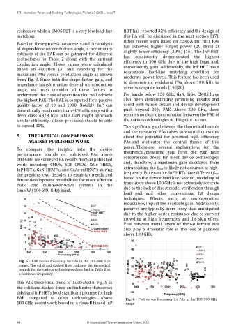
Fig. 5 - PAE versus frequency for PAs in the 100-300 GHz
range. The solid and dashed lines indicate the theoretical
bounds for the various technologies described in Table 2 as
a funtion of frequency.
The PAE theoretical trend is illustrated in Fig. 5 as
the solid and dashed lines and indicates that across
this band InP HBTs hold significant promise for high
PAE compared to other technologies. Above Fig. 6 - Psat versus frequency for PAs in the 100-300 GHz
100 GHz, recent work based on a class-B biased InP range
44 © International Telecommunication Union, 2021