
Page 54 - ITU Journal Future and evolving technologies Volume 2 (2021), Issue 7 – Terahertz communications
P. 54
ITU Journal on Future and Evolving Technologies, Volume 2 (2021), Issue 7
underlying device technology. The PAE can be network. Moreover, as one moves from LmmW
expressed in terms of several factors. bands at 60 GHz to the UmmW bands at 140 and
220 GHz, the optimum conduction angle moves
1 V K Q o
PAE = η (1 − ) (1 − ) ( ) (3) away from class B bias towards the class A bias. The
G V DD Q o +Q t
maximum possible PAE drops from more than 40%
The PAE depends on the drain efficiency, , the to 30% at 140 GHz. When the PA design targets
operating gain of the PA (G), the knee (VK) and 220 GHz, the maximum PAE becomes around 17%.
supply voltage (VDD) of the device, and the loss
factor for matching the load line of the device to the
load impedance, which is expressed above in terms
of a impedance transformation quality factor, (Qt),
and passive element quality factor (Qo).
Consequently, the knee voltage relative to the
supply voltage imposes a penalty on the available
PAE. Additionally, the impedance transformation
between the load line of the transistor and the
output impedance, e.g. 50 Ohms, reduces the
maximum efficiency.
The drain efficiency is determined by the biasing of
the PA as well as the harmonic tuning at the load.
With only matching of the load line of the device to
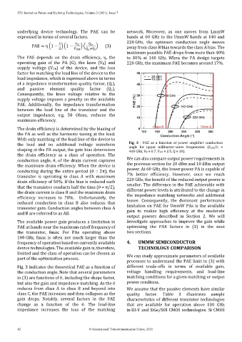
the load and no additional voltage waveform Fig. 3 - PAE as a function of power amplifier conduction
angle for upper millimeter-wave frequencies. (fmax/fT =
shaping at the PA output, the gate bias determines 400 GHz, VK = 0.7, VDD = 2.5, Q = 10).
the drain efficiency as a class of operation. The
conduction angle, , of the drain current captures We can also compare output power requirements in
the maximum drain efficiency. When the device is the previous section for 20 dBm and 10 dBm output
conducting during the entire period ( = 2π), the power. At 60 GHz, the lower power PA is capable of
transistor is operating in class A with maximum 7% better efficiency. However, once we reach
drain efficiency of 50%. If the bias is reduced such 220 GHz, the benefit of the reduced output power is
that the transistor conducts half the time ( = π/2), smaller. The difference in the PAE achievable with
the drain current is class B and the maximum drain different power levels is attributed to the change in
efficiency increases to 78%. Unfortunately, the the impedance matching networks and additional
reduced conduction in class B also reduces that losses. Consequently, the dominant performance
transistor gain. Conduction angles between class A limitation on PAE for UmmW PAs is the available
and B are referred to as AB. gain to realize high efficiency at the moderate
output powers described in Section 2. We will
The available power gain produces a limitation in investigate approaches to improve the gain while
PAE at bands near the maximum cutoff frequency of optimizing the PAE factors in (3) in the next
the transistor, fmax. For PAs operating above two sections.
100 GHz, fmax is often not much larger than the
frequency of operation based on currently available 4. UMMW SEMICONDUCTOR
device technologies. The available gain is, therefore, TECHNOLOGY COMPARISON
limited and the class of operation can be chosen as We can study approximate parameters of available
part of the optimization process.
processes to understand the PAE limit in (3) with
Fig. 3 indicates the theoretical PAE as a function of different trade-offs in terms of available gain,
the conduction angle. Note that several parameters voltage handling requirements, and load-line
in (3) are functions of including the shape factor, matching conditions for a given matching or output
but also the gain and impedance matching. As the power condition.
reduces from class A to class B and beyond into We assume that the passive elements have similar
class C, the PAE increases and then collapses as the quality factor. Table 1 illustrates sample
gain drops. Notably, several factors in the PAE characteristics of different transistor technologies
change as a function of the . The load-line that are available for operation above 100 GHz
impedance increases the loss of the matching in III-V and SiGe/SOI CMOS technologies. Si CMOS
42 © International Telecommunication Union, 2021