
Page 126 - ITU Journal Future and evolving technologies – Volume 2 (2021), Issue 2
P. 126
ITU Journal on Future and Evolving Technologies, Volume 2 (2021), Issue 2
Node k
TX RF Chain 1 TX 1
Upsample RX 1
Pulse Shape DAC PA
Upconversion Downlink channel
Node q
TX RF Chain TX
Upsample RX
Pulse Shape DAC PA
Upconversion
TX Digital
Beamforming
Self-interference Inter-node interference
Joint Cancellation channel channel
and Beamforming
Design
Analog
Canceller
RX Digital
Beamforming RX RF Chain 1 RX 1 TX 1
Matched Filter
Downsample ADC LNA
Downconversion Adder 1 Uplink channel
Node m
RX RF Chain RX
Matched Filter TX
Downsample ADC LNA
Downconversion Adder
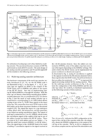
Fig. 1 – Schematic diagram of the considered system model and the proposed FD MIMO architectural components. The FD MIMO node communicates
with the two half duplex multi‑antenna nodes and , the former in the downlink and the latter in the uplink communications. Node incorporates
processing blocks dedicated to TX and RX digital BF, analog SI cancellation, as well as to the joint design of analog cancellation and TX/RX digital BF.
the utilization of analog taps and is thus labeled as multi‑ the ‑th RX antenna element. Since the adders are con‑
tap canceler. The second architecture consists of AUX TXs nected to DEMUXs, some of the adders may have zero in
and termed as multi‑AUX‑TX canceler. The joint design of one of the inputs depending on the DEMUXs’ settings. The
the analog canceler parameters and TX and RX digital BF adders before the RX RF chains can be implemented via
will be detailed in the following sections. power combiners or directional couplers.
As illustrated in Fig. 2, analog SI cancellation is applied
3.1 Multi‑tap analog canceler architecture to the signals received at the RX antenna elements before
these signals enter the RX RF chains. Recall from Section 2
The hardware components of the multi‑tap canceler, ini‑ that we utilize the notation C ∈ ℂ × to represent the
tially introduced in [17, 19], for the FD MIMO node signal processing realized by the analog canceler. Thus,
are illustrated in Fig. 2. In this igure, ≤ can‑ for the multi‑tap canceler architecture in Fig. 2, C cap‑
celer taps are applied via MUXs to the outputs of the tures the con iguration of the MUXs/DEMUXs and the can‑
TX RF chains and via DEMUXs and adders to the inputs celer tap values. We model C in baseband representation
of the RX RF chains. One way of implementing ana‑ as the following cascade of three matrices:
log RF MUXs/DEMUXs is through RF switches. With the C ≜ L L L , (6)
term ‘tap’ we denote a ixed delay‑variable phase shifter‑ 3 2 1
variable attenuator line, as considered in [15]. It is shown where L ∈ ℝ × , L ∈ ℂ × , and L ∈ ℝ × . The
3
1
2
in Fig. 2 that the input of each analog canceler tap is elements [L ] with = 1, 2, … , and = 1, 2, … , ,
1 ,
connected to a corresponding ‑to‑1 MUX which allows and [L ] with = 1, 2, … , and = 1, 2, … , take
3 ,
routing of any of the TX RF chain signals to the input the binary values 0 or 1, and it must hold that:
of the tap. The connection from each TX RF chain to each
MUX input can be done via power dividers or directional ∑[L ] = 1 ∀ = 1, 2, … , ,
couplers [15]. The signal that inputs to a tap undergoes 1 , (7a)
=1
a delay, phase shift, and attenuation, and this generates
as an output an analog cancellation signal. The output of
each tap is connected to a 1‑to‑ DEMUX, which routes ∑[L ] = 1 ∀ = 1, 2, … , . (7b)
3 ,
the cancellation signal at the output of the tap to one of =1
the adders located just before the RX RF chains. There The ‑th row of L indicates the MUX con iguration at the
1
is a total of such adders and we use “Adder , ” to input of the ‑th tap of the canceler, while the ‑th column
label the adder that connects DEMUX to RX RF chain . of L shows the DEMUX con iguration at the output of the
3
Thus, the signal input to the ‑th RX RF chain is the result ‑th tap of the canceler. The L in (6) is a diagonal ma‑
2
of adding cancellation signals to the signal received at trix whose complex entries represent the attenuation and
112 © International Telecommunication Union, 2021