
Page 182 - Proceedings of the 2017 ITU Kaleidoscope
P. 182
2017 ITU Kaleidoscope Academic Conference
In order to provide a common development environment,
the standard proposes the discrete-event and open source
network simulator denoted as NS-3 to integrate all the
aforementioned steps and components. The objective is that
future investigation in the field of nanoscale
communications has a starting point for exploiting all the
power of the IEEE P1906.1 standard. To this purpose, the
simulator follows a hierarchical modular structure, dividing
the EM communication implementation into two groups;
both taking into account the guidelines of the standard.
Specifically, the first group develops the five main
framework components, while the second implements other
secondary entities involved in the communication process
but not classified as “components” (i.e., communication
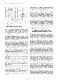
Figure 2. EM communication reference model interface, transmitter communication interface, receiver
communication interface, medium, and net nanodevice). It
is worth remarking that the software developed under the
2.4. EM communication reference model NS3 simulator supports the interaction of all these modules,
offering a complete communication scheme.
Figure 2 illustrates the general communication reference
model of the standard extended to EM communications. 3. IEEE P1906.1 STANDARD WEAKNESSES
Also, the sequence of steps followed to carry out a IDENTIFIED FOR EM COMMUNICATIONS
communication between two nanodevices (in that order) is
displayed. They are enumerated and commented on in the Once the main features of the IEEE P1906.1 standard have
following paragraphs. been introduced, we identified several aspects which make
1) The sender nanodevice receives a message from the the standard excessively open or even a not well-defined
upper layers, in particular, a string of bits encoding the approach. In this section, we discuss some of the issues not
message to be dispatched. This message is delivered to the thoroughly covered by the standard.
Transmitter Communication Interface. First of all, we should indicate the difficulty of giving a
2) The Perturbation component generates the message general definition of the concept “nanoscale communication
carrier, considering parameters characterizing the EM network”, since it requires the inclusion of requirements
transmission, for instance, the central frequency in the THz from two different scientific fields, namely Molecular and
band to transmit, the bandwidth (usually from 0.55 THz to EM. They are so different, that concepts such as “network”
1.55 THz), the transmission power, pulse features, type of and “communication” may have different meanings in each
modulation, etc. Regarding modulation, the Time-Spread discipline. In addition, in order to maintain the generality of
On-Off Keying (TS-OOK) modulation is the most widely the definition, a communication system is considered at the
extended because it is a straightforward scheme that sharply nanoscale when one or more essential system components
decreases the implementation complexity, alleviating the are sized at nanometers in at least one dimension. Actually,
processing and computing tasks of nanodevices. following the guidelines of this definition, most works
3) The Transmitter Communication Interface triggers the already published about EM nanocommunications [6], [8],
propagation in the physical medium by passing through the [9], [13] (and therefore, prior to the IEEE P1906.1 standard
Message Carrier, Perturbation, and Field components. -draft- was launched) would be included under the umbrella
Regarding this last component, an omnidirectional antenna of the standard, since antennas employed in these studies
is employed. are at the nanoscale. In detail, as can be seen in Table 2
4) The Motion component is created in function of the (extracted from [10]), the THz waves radiated by graphene
propagation model in the scenario under consideration (e.g. or CNT antennas are both considered “components below
the human body), and takes into account requirements such 100 nm” and therefore “non-standard physics”. So, although
as path loss or background noise [12] to modify properties these studies built their designs from microscale electronic
of the message carrier, for instance, propagation loss or devices (and thus, the resulting design is at the microscale),
end-to-end delay. the employment of THz waves as message carriers is
5) The receiver Specificity component checks and verifies enough to consider the communication at the nanoscale. As
that all the aforementioned parameters stored within the can be observed, the concept of “nanoscale communication
received message carrier are the same as those contained in network”, is diffuse enough to consider microdevices
the receiver Perturbation component. operating in a nanonetwork.
6) In the case that step 5) is correctly carried out, the Concerning the physical level, the restrictions on the
message carrier is delivered to the receiver nanodevice. amount of available energy in each nanodevice (we name
7) Finally, the message is dispatched to the upper layers of them nanodevices, although their dimensions may be at the
microscale) has an important impact on the communication
the receiver.
– 166 –